A Handful of Chips, Lightly Nuked
Written and Photographed by Sid Perkins of the Missourian Staff
This story appeared in the "Frontiers" section (page 5A)
of the Columbia Missourian on December 3, 1996.
In a game of word association, the phrase "nuclear reactor" could likely elicit a response of "nuclear waste." Other than the electricity or steam energy produced by a nuclear reactor, many people would be hard pressed to think of a beneficial byproduct of a nuclear reaction.
Yet at the University of Missouri Research Reactor Center, known as MURR, the same subatomic particles that enable a nuclear chain reaction are used to generate a product that is vital in today's high-tech world: semiconductors.
In some cases, exposure to the intense radioactivity near the core of a nuclear reactor is the only way to achieve the degree of quality control required to consistently produce the semiconductor material.
It's possible that the material in some of the chips in your computer's circuit boards has spent time near the core of a nuclear reactor. But don't panic: The material is not radioactive now, so there's simpy no reason to stretch your keyboard coard out to its full length and sit far away from the computer.
MURR is just one of the reactors around the world that commercially exploits the radiation that is normally considered a dangerous byproduct of a reactor's operation, and they do it on a grand scale. MURR processes nearly 29,000 pounds of semiconductor material annually.
"In a year's time, we do roughly 13 metric tons," said Kathy Sanford, project specialist at MURR. "However, that amount can range between 7 and 16, depending on what specifications the customer wants."
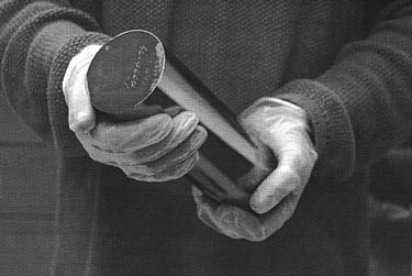
The material processed at MURR eventually ends up in computer chips and other semiconductor devices. It arrives at the reactor, however, in a far different form: ingots of extremely pure silicon which have been milled into cylinders with diameters between 2 and 6 inches.
Sanford describes the material as "11 nines pure," which means that the material is 99 percent, plus another 11 nines after the decimal point, silicon. In other words, only one atom of every 10,000,000,000,000 - that's 100 trillion - in the ingots is not a silicon atom.
At that degree of purity, silicon doesn't conduct electricity because almost all of the electrons in the material are locked into the chemical bonds between atoms. What transforms the silicon from a nonconductor to a semiconductor is added impurities that contribute electrons that are free to move through the material and conduct electricity.
Adding impurities, or "doping," can be done two ways, said Steve Gunn, reactor services engineer at MURR. One method is to melt the silicon and then physically mix in the impurities before the silicon recrystallizes into a solid. Gunn points out this method usually results in lower quality control for the final product, especially in cases where very low amounts of impurities need to be added to the silicon.
An alternate method, which is called neutron transmutation doping, or NTD, exposes the silicon to intense radiation.
"The silicon ingots are lowered to within 7 to 9 inches from the core," Sanford said of the process used at MURR. "As far as time in the reactor, it can be as short as 20 minutes or as long as 60 hours, depending upon the specifications set by the customer and the irradiation position where the ingot is placed."
The atoms of silicon in the ingot undergo changes when they absorb some of the radioactivity that escapes from the core of the reactor. The most common reaction is when a silicon atom that has an atomic weight of 30 absorbs aneutron, becomes unstable and then radioactively decays into a phosphorus atom, Sanford said.
After the radioactive decay, the new phosphorus atom has one more electron than the silicon atom did. It is these new phosphorus atoms, and their extra electrons, that transform the silicon material into a semiconductor.
Under each contract for irradiation services, MURR's customers usually specify a target resistivity for the irradiated material, Sanford said. Resistivity is a measure of a material's resistance to the flow of electricity. As the number of phosphorus atoms in the irradiated material increases, the ability to conduct electricity increases and the resisitivity drops.
"There's a calibration factor that links the distance from the reactor core, the radiation counts, the target resistivity for that particular order, and the time of irradiation exposure," Sanford said.
"Essentially, we just load it in, expose it for a certain amount of time, and then we ship the irradiated material back to the customer after we test it to ensure residual radioactivity has dropped below acceptable levels."


MURR has captured about 50 percent to 60 percent of the world market for the irradiation of 3-inch-diameter ingots of silicon, Sanford said, adding their irradiation process is economical for a number of reasons.
"In addition to being a university reactor, the process we've developed isn't really complicated," she said. "It doesn't require a lot of highly sensitive equipment, other than the detectors that are located within the reactor, so we've been able to keep our real costs down."
In addition to favorable costs, the NTD method of introducing impurities into silicon improves quality control compared to conventional doping methods, Gunn said.
Conventional doping works well in the production of lower-resistivity materials, where higher amounts of phosphorus or other impurities are called for, Gunn said. But higher resistivities call for very small amounts of impurities, and that's where the NTD method used at MURR is indispensable.
"At high resistivities, it's pretty much impossible to do by conventional doping," he said. "You're talking about so few atoms in there. You might wind up with 500 atoms on one side of the wafer and 200 on the other, so distribution is really a problem (with conventional doping.) But irradiation is a totally random event, and with NTD you get the phosphorus atoms spread evenly throughout the material."
After the ingots of silicon are irradiated at MURR they are returned to the customers for further processing. The ingots are sliced into wafers, circuits are etched upon their surface, and then individual semiconductor devices are trimmed from the small discs and incorporated into larger components.
Although MURR is processing fewer irradiation orders this year, Sanford explains that this is a short-term situation resulting from a temporary oversupply of irradiated silicon.
"The Japanese market is in a bit of a decline right now, because they had anticipated an event which would drive up the demand for material," she said. "So they did a little bit of stockpiling, but then the event didn't come."
Once the oversupply has been consumed and the demand for irradiated silicon returns, MURR hopes to increase their orders and capture even more of the market for the irradiation of 3-inch material.
"Now there is a shift from smaller diameters to larger diameters," Sanford said. "We sort of have a niche in that market because most of the other reactors have discontinued their use of the 3-inch irradiation spaces and are doingf the larger diameter.
"I think that more of the world's capacity will shift to us because we are an economic supplier of that material, and we do have such a history in the market."
Glossary of Terms
- Doping
The addition of trace elements to silicon to transform it into a semiconductor.
- Ingot
A bar or other convenient shape of processed material.
- Irradiation
The exposure of a material to some type of radiation.
- Semiconductor
A substance whose electrical conductivity is normally poor but is improved by the addition of small amounts of other substances.
---[
Copyright 1996 by Missourian Publishing Association Inc.
All rights reserved.
---[